Research

Atomic layer deposition (ALD) thin film materials research
Atomic layer deposition (ALD) is a thin film deposition technique closely related to Chemical Vapour Deposition (CVD). Unlike CVD, ALD relies on self-limiting cyclic surface reactions that provide exquisite control over the thin film growth process. ALD is a surface chemistry driven process utilising alternating pulses of complementary precursor gases. The process involves surface exchange reactions between chemisorbed metal-containing precursors and nucleophilic co-reactants such as –OH, -NH or -SH. The reactants are separated by gas purges to suppress unwanted gas phase reactions, hence, ALD proceeds via self-limiting steps. The self limiting nature of ALD offers opportunities to accurately produce ultra thin coatings with sub-nanometre control of thickness & composition, exceptional uniformity and conformity even on high aspect ratio three dimensional microstructures. In addition, ALD processes can often be run at low temperatures allowing coatings onto temperature sensitive substrates. Although ALD has been around for almost half a century, Worldwide interest from the research community only really started to grow in the late-1990’s driven by the microelectronics industry. Over the last decade, ALD has been recognized as an enabling technology for an increasingly diverse range of research and manufacturing areas ranging from microelectronics, optoelectronics, photonics and energy storage/generation through to micro-machines (MEMS), bio-medical devices, food packaging, decorative coatings and even high energy explosives.
My key areas of interests relating to ALD:
- ALD processes: Developing new ALD processes, particularly for novel/advanced functional thin film materials.
- Precursor delivery: Developing methodologies for transport 'difficult' precursors.
- In-situ analysis techniques to probe ALD process chemistry: Gaining a fundamental insight into the surface chemistry and kinetics of different ALD process with the aim of using this knowledge to advance the field of research.
- Physico-chemical characterisation: Using techniques such as XRD, AFM, SEM, XPS, EDX, MEIS and Raman to correlate growth conditions with the resulting physico-chemical properties of the films.
- Functional characterisation: Assessing the functional (electrical, optical, biological, catalytic, etc) properties of the thin film materials.

Applications of thin film materials
ALD is a truly enabling technology with a vast range of potential applications in a diverse range of technology sectors. Much of my research is driven by the desire to exploit functional thin film coatings (produced primarily by ALD, but also by other techniques such as MOCVD & PVD) to enhance existing technology and to enable the development of new technology. Ultra-thin coatings can have a remarkable impact on the performance of existing technology, while also opening the door for the development of new technology.
In recent years, I have been involved in collaborative research spanning a number of technology sectors. For example:
- Microelectronics: High-k dielectrics for silicon microelectronics
- Microelectronics: GaN-on-Si high electron mobility transistors (HEMT)
- Microelectronics: Resistive switching memory devices
- Microelectronics: ALD of nitrides
- Microelectronics: Zn-oxide based thin-film transistors (TFTs)
- Photo-voltaics: Transparent conducting oxides
- Solar-fuels: Hematite photo anodes for active water splitting
- Battery technology: Coatings to enhance Li-ion battery lifetime
- Bio-medical: Antimicrobial silver coatings for bio-medical implants
- Optics: Coatings for advanced optical components
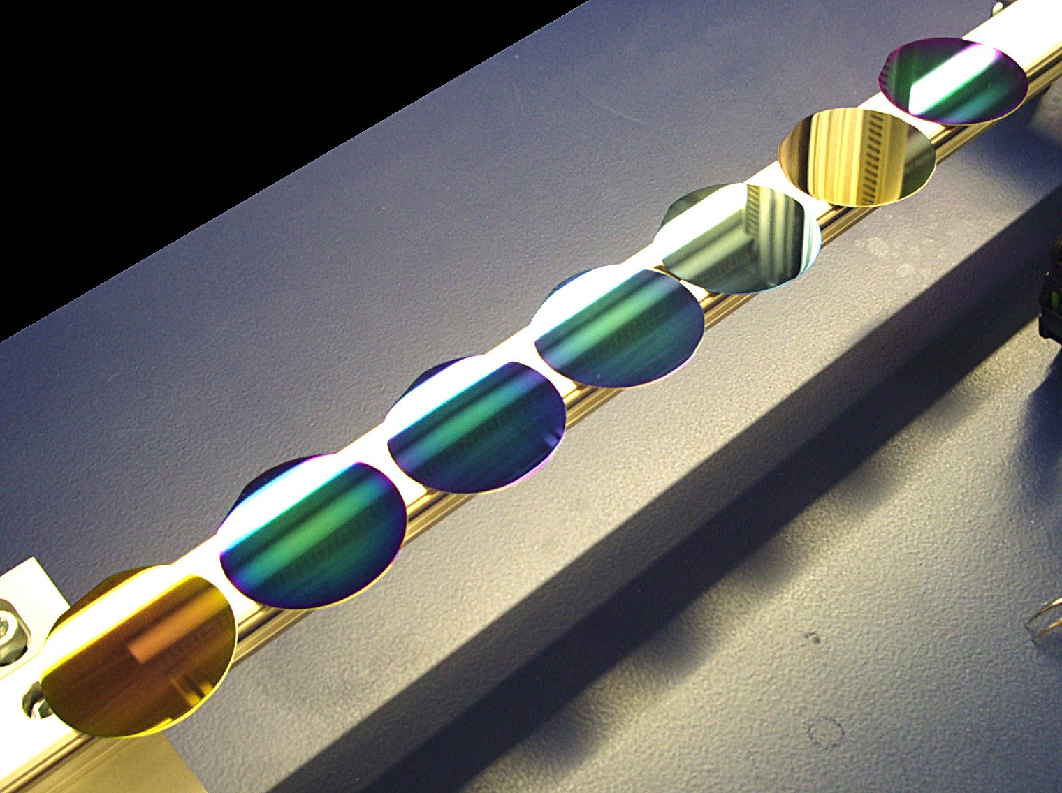
- Optics: High volume fabrication of laser targets using MEMS techniques
Research grants
Additional Supplement HEIF Allocation 2020-21
RESEARCH ENGLAND (UK)
August 2020 - July 2021
Manufacturing with Light 2: photochemical ALD to manufacture functional thin films.
ENGINEERING & PHYSICAL SCIENCES RESEARCH COUNCIL
December 2015 - December 2018
An in-situ LEIS facility for atomic-scale assembly manufacturing research
ENGINEERING & PHYSICAL SCIENCES RESEARCH COUNCIL
June 2016 - October 2017
Atomic layer deposition of Hafnium-nitride and Lanthanide nitrides
ENGINEERING & PHYSICAL SCIENCES RESEARCH COUNCIL
October 2007 - March 2011
Liquid injection ALD of Cp- based precursers for deposition of dielectric materials.
ENGINEERING & PHYSICAL SCIENCES RESEARCH COUNCIL
October 2006 - October 2009
KEL11/26 - Development of ALD coating processes and materials to promote bone in-growth into SLM built bio-medical implants
ENGINEERING & PHYSICAL SCIENCES RESEARCH COUNCIL
November 2011 - September 2012
Manufacturing with Light - photochemical ALD to manufacture functional thin films
ENGINEERING & PHYSICAL SCIENCES RESEARCH COUNCIL
March 2014 - August 2015
Mechanisms and Control of Resistive Switching in Dielectrics
ENGINEERING & PHYSICAL SCIENCES RESEARCH COUNCIL
January 2015 - January 2018
Small items of Research Equipment at the University of Liverpool
ENGINEERING & PHYSICAL SCIENCES RESEARCH COUNCIL
November 2012 - March 2013
Research collaborations
Alex Cowan
Dr
ALD coatings to enhance photo-anodes and photo-cathodes
Paul R. Chalker
Prof.
Developing deposition processes for the fabrication of oxide thin films and superlattices.
Frank Jaeckel
Dr
ALD coatings to enhance the performance and lifetime of photocathodes for solar fuels.
Sudhiranjan Tripathy
Dr
IMRE - A*Star (Singapore)
ALD of high-k dielectrics for GaN-on-Silicon based MOS-HEMT's
Christopher Mitchell
Dr
University of Ulster
Anti-microbial coatings by ALD for bio-medical implants
Prof. Aimin Song
Prof.
University of Manchester, UK
This collaboration was set-up in December 2009 to explore the potential of using ALD coatings as the basis for Prof. Songs novel nanoelectronic devices.
Chris Sutcliffe
Dr
Anti-microbial coatings by ALD for bio-medical implants
Helen Aspinall
Dr
The development of new precursors for MOCVD and ALD
Steve Taylor
Prof.
Developing new high-k dielectric oxides for silicon electronics.
A.C. Jones
The development of new precursors for MOCVD of oxide thin films for silicon electronics.