Successful HV-CMOS sensor test beam at DESY with Liverpool Crew
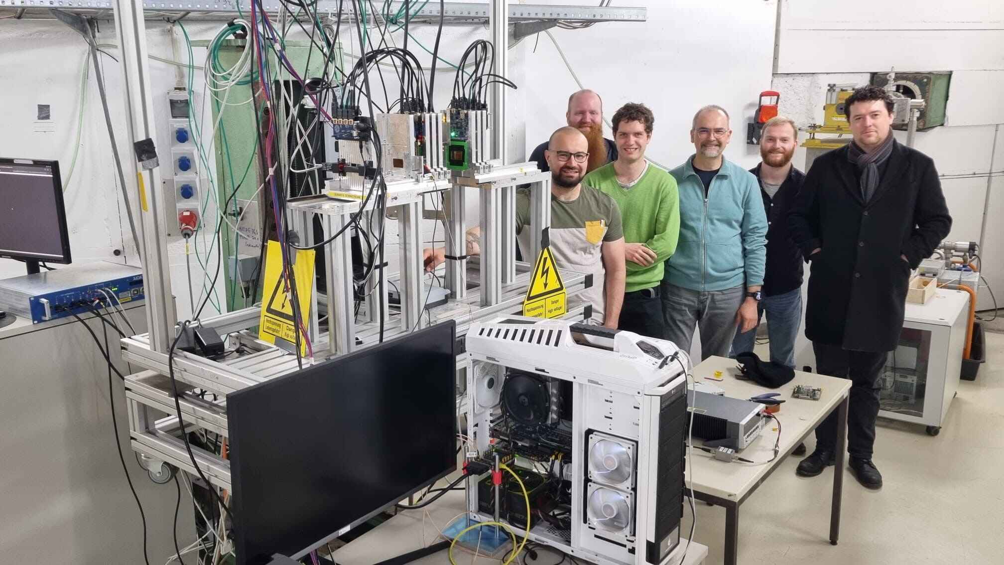
Photo Credit: Christian Irmler
The RD50-MPW prototypes are High-Voltage CMOS pixel chips in the 150 nm technology from LFoundry S.r.l. The aim is to develop thin monolithic silicon sensors with excellent radiation tolerance, fast timing resolution and high granularity to meet the challenging tracking targets of future physics experiments. The design effort of these pixel chips is led by Liverpool (Chenfan Zhang, Sam Powell, Jan Hammerich and Eva Vilella) within the CERN-RD50 collaboration.
RD50-MPW4, the latest prototype within this programme, implements significant improvements for a high breakdown voltage (> 400 V), and therefore an excellent radiation tolerance, through a multiple ring structure around the chip edge. A subset of the fabricated samples was processed after fabrication to enable substrate backside-biasing to high voltage and achieve further radiation tolerance improvements. The chip was delivered in February and evaluated in the Liverpool clean rooms and other CERN-RD50 institutes.
A test beam was conducted at DESY in April 2024 to fully test this new prototype. It focussed on evaluating the non-irradiated samples with a beam of electrons, using a custom built Data Acquisition System. It had important contributions from our own engineer (and PhD student) Sam Powell and PhD student Ben Wade. Both the unprocessed and processed samples biased to very high voltages were tested. Preliminary results show a better than 99.99% efficiency. The bulk of the analysis of the more than 1 TB test beam data is ongoing. A future test beam, most likely in the autumn, will follow and concentrate on evaluating samples irradiated with neutrons to very high fluence (up to 3x10¹⁶ neq/cm2). The processed samples with backside-biasing are expected to show much better results than the topside biased samples, especially after irradiation.